Simple Serial Shift Register Truth Table
The registers which will shift the bits to right are called “Shift right registers”. Example: If we pass the data 1101 to the data input, the shifted output will be 0110. This one is the simplest register among the four types. As the clock signal is connected to all the 4 flip flops. A serial adder consists of a 1-bit full-adder and several shift registers. In serial adders, pairs of bits are added simultaneously during each clock cycle. Two right-shift registers are used to hold the numbers (A and B) to be added, while one left-shift register is used to hold the sum (S).
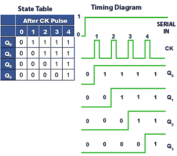
In Serial In Parallel Out (SIPO) shift registers, the data is stored into the register serially while it is retrieved from it in parallel-fashion. Figure 1 shows an n-bit synchronous SIPO shift register sensitive to positive edge of the clock pulse. Here the data word which is to be stored (Data in) is fed serially at the input of the first flip-flop (D1 of FF1). It is also seen that the inputs of all other flip-flops (except the first flip-flop FF1) are driven by the outputs of the preceding ones say for example, the input of FF2 is driven by the output of FF1. In this kind of shift register, the data stored within the register is obtained as a parallel-output data word (Data out) at the individual output pins of the flip-flops (Q1 to Qn).
In general, the register contents are cleared by applying high on the clear pins of all the flip-flops at the initial stage. After this, the first bit, B1 of the input data word is fed at the D1 pin of FF1.
This bit (B1) will enter into FF1, get stored and thereby appears at its output Q1 on the appearance of first leading edge of the clock. Further at the second clock tick, the bit B1 right-shifts and gets stored into FF2 while appearing at its output pin Q2 while a new bit, B2 enters into FF1. Similarly at each clock tick the data within the register moves towards right by a single bit while a new bit of the input word enters into the register. Meanwhile one can extract the bits stored within the register in parallel-fashion at the individual flip-flop outputs.
Analyzing on the same grounds, one can note that the n-bit input data word is obtained as an n-bit output data word from the shift register at the rising edge of the nth clock pulse. This working of the shift-register can be summarized as in Table I and the corresponding wave forms are given by Figure 2.
In the right-shift SIPO shift-register, data bits shift from left to right for each clock tick. However if the data bits are made to shift from right to left in the same design, one gets a left-shift SIPO shift-register as shown by Figure 3. Nevertheless the basic working principle remains the same except the fact that now Bn down to B1 is stored in Qn down to Q1 i.e. Q1 = B1, Q2 = B2 … Qn = Bn at the nth clock tick.
- Digital Circuits Tutorial
- Digital Circuits Resources
- Selected Reading
We know that one flip-flop can store one-bit of information. In order to store multiple bits of information, we require multiple flip-flops. The group of flip-flops, which are used to hold (store) the binary data is known as register.
If the register is capable of shifting bits either towards right hand side or towards left hand side is known as shift register. An ‘N’ bit shift register contains ‘N’ flip-flops. Following are the four types of shift registers based on applying inputs and accessing of outputs.
- Serial In − Serial Out shift register
- Serial In − Parallel Out shift register
- Parallel In − Serial Out shift register
- Parallel In − Parallel Out shift register
Serial In − Serial Out (SISO) Shift Register
The shift register, which allows serial input and produces serial output is known as Serial In – Serial Out (SISO) shift register. The block diagram of 3-bit SISO shift register is shown in the following figure.
This block diagram consists of three D flip-flops, which are cascaded. That means, output of one D flip-flop is connected as the input of next D flip-flop. All these flip-flops are synchronous with each other since, the same clock signal is applied to each one.
In this shift register, we can send the bits serially from the input of left most D flip-flop. Hence, this input is also called as serial input. For every positive edge triggering of clock signal, the data shifts from one stage to the next. So, we can receive the bits serially from the output of right most D flip-flop. Hence, this output is also called as serial output.
Example
Let us see the working of 3-bit SISO shift register by sending the binary information “011” from LSB to MSB serially at the input.
Assume, initial status of the D flip-flops from leftmost to rightmost is $Q_{2}Q_{1}Q_{0}=000$. We can understand the working of 3-bit SISO shift register from the following table.
| No of positive edge of Clock | Serial Input | Q2 | Q1 | Q0 |
|---|---|---|---|---|
| 0 | - | 0 | 0 | 0 |
| 1 | 1(LSB) | 1 | 0 | 0 |
| 2 | 1 | 1 | 1 | 0 |
| 3 | 0(MSB) | 0 | 1 | 1(LSB) |
| 4 | - | - | 0 | 1 |
| 5 | - | - | - | 0(MSB) |
The initial status of the D flip-flops in the absence of clock signal is $Q_{2}Q_{1}Q_{0}=000$. Here, the serial output is coming from $Q_{0}$. So, the LSB (1) is received at 3rd positive edge of clock and the MSB (0) is received at 5th positive edge of clock.
Therefore, the 3-bit SISO shift register requires five clock pulses in order to produce the valid output. Similarly, the N-bit SISO shift register requires 2N-1 clock pulses in order to shift ‘N’ bit information.
Serial In - Parallel Out (SIPO) Shift Register
The shift register, which allows serial input and produces parallel output is known as Serial In – Parallel Out (SIPO) shift register. The block diagram of 3-bit SIPO shift register is shown in the following figure.
This circuit consists of three D flip-flops, which are cascaded. That means, output of one D flip-flop is connected as the input of next D flip-flop. All these flip-flops are synchronous with each other since, the same clock signal is applied to each one.
In this shift register, we can send the bits serially from the input of left most D flip-flop. Hence, this input is also called as serial input. For every positive edge triggering of clock signal, the data shifts from one stage to the next. In this case, we can access the outputs of each D flip-flop in parallel. So, we will get parallel outputs from this shift register.
Example
Let us see the working of 3-bit SIPO shift register by sending the binary information “011” from LSB to MSB serially at the input.
Assume, initial status of the D flip-flops from leftmost to rightmost is $Q_{2}Q_{1}Q_{0}=000$. Here, $Q_{2}$ & $Q_{0}$ are MSB & LSB respectively. We can understand the working of 3-bit SIPO shift register from the following table.
| No of positive edge of Clock | Serial Input | Q2(MSB) | Q1 | Q0(LSB) |
|---|---|---|---|---|
| 0 | - | 0 | 0 | 0 |
| 1 | 1(LSB) | 1 | 0 | 0 |
| 2 | 1 | 1 | 1 | 0 |
| 3 | 0(MSB) | 0 | 1 | 1 |
The initial status of the D flip-flops in the absence of clock signal is $Q_{2}Q_{1}Q_{0}=000$. The binary information “011” is obtained in parallel at the outputs of D flip-flops for third positive edge of clock.
So, the 3-bit SIPO shift register requires three clock pulses in order to produce the valid output. Similarly, the N-bit SIPO shift register requires N clock pulses in order to shift ‘N’ bit information.
Parallel In − Serial Out (PISO) Shift Register
The shift register, which allows parallel input and produces serial output is known as Parallel In − Serial Out (PISO) shift register. The block diagram of 3-bit PISO shift register is shown in the following figure.
This circuit consists of three D flip-flops, which are cascaded. That means, output of one D flip-flop is connected as the input of next D flip-flop. All these flip-flops are synchronous with each other since, the same clock signal is applied to each one.
In this shift register, we can apply the parallel inputs to each D flip-flop by making Preset Enable to 1. For every positive edge triggering of clock signal, the data shifts from one stage to the next. So, we will get the serial output from the right most D flip-flop.
Example
Let us see the working of 3-bit PISO shift register by applying the binary information “011” in parallel through preset inputs.
Since the preset inputs are applied before positive edge of Clock, the initial status of the D flip-flops from leftmost to rightmost will be $Q_{2}Q_{1}Q_{0}=011$. We can understand the working of 3-bit PISO shift register from the following table.
| No of positive edge of Clock | Q2 | Q1 | Q0 |
|---|---|---|---|
| 0 | 0 | 1 | 1(LSB) |
| 1 | - | 0 | 1 |
| 2 | - | - | 0(LSB) |
Here, the serial output is coming from $Q_{0}$. So, the LSB (1) is received before applying positive edge of clock and the MSB (0) is received at 2nd positive edge of clock.
Therefore, the 3-bit PISO shift register requires two clock pulses in order to produce the valid output. Similarly, the N-bit PISO shift register requires N-1 clock pulses in order to shift ‘N’ bit information.
Parallel In - Parallel Out (PIPO) Shift Register
The shift register, which allows parallel input and produces parallel output is known as Parallel In − Parallel Out (PIPO) shift register. The block diagram of 3-bit PIPO shift register is shown in the following figure.
This circuit consists of three D flip-flops, which are cascaded. That means, output of one D flip-flop is connected as the input of next D flip-flop. All these flip-flops are synchronous with each other since, the same clock signal is applied to each one.
Chapter 1 Getting Started with LabVIEW Virtual Instruments Getting Started with LabVIEW 1-20 ni.com. This chapter introduced the following keyboard shortcuts. Note The key in shortcuts corresponds to the (Mac OS) or key or (Linux) key. .Self- taught.LabVIEW is a (massive) package. To expand.You’ve got - exactly - what you need.Essentially if you are running any experiment and want to save time/money. What is LabVIEW? Wiki definition: LabVIEW is a system-design platform and development. A guide to strengths and uses presented by Dummies. That seems pretty short to me for a 9600 baud serial com. Unfortunately, most readers of this Forum, including some real Experts, have not mastered the skill of being able to read the code that Posters fail to post. Serial time out labview for dummies. How to write and read data from PC serial port and interfacing with devices such as PIC microcontrollers. Tools: NI LabVIEW Virtual Serial Ports Emulator (VSPE) Serial terminal from MickroC IDE.
In this shift register, we can apply the parallel inputs to each D flip-flop by making Preset Enable to 1. We can apply the parallel inputs through preset or clear. These two are asynchronous inputs. That means, the flip-flops produce the corresponding outputs, based on the values of asynchronous inputs. In this case, the effect of outputs is independent of clock transition. So, we will get the parallel outputs from each D flip-flop.
Example
Let us see the working of 3-bit PIPO shift register by applying the binary information “011” in parallel through preset inputs.
Since the preset inputs are applied before positive edge of Clock, the initial status of the D flip-flops from leftmost to rightmost will be $Q_{2}Q_{1}Q_{0}=011$. So, the binary information “011” is obtained in parallel at the outputs of D flip-flops before applying positive edge of clock.
Therefore, the 3-bit PIPO shift register requires zero clock pulses in order to produce the valid output. Similarly, the N-bit PIPO shift register doesn’t require any clock pulse in order to shift ‘N’ bit information.